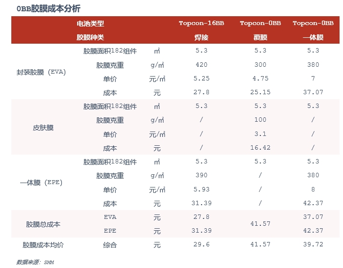
In traditional welding methods, further thinning of silicon wafer welding strips poses a risk of grid breakage, and further thinning of encapsulation film weight is challenging. Currently, the cost of skin film is around 3 yuan/㎡, but it still requires pairing with encapsulation film, which has a high cost. With future mass production and technological optimization, costs are expected to decrease further. The paired encapsulation film has currently been reduced to 200g/㎡ and is still in the testing phase, with some sample modules being tested by component manufacturers. The one-piece film, extruded in a single process, has a lower cost compared to the combination of skin film and encapsulation film. Currently, First, Betterial, Sveck, and Lushan are leading in R&D. First's CH(15) and CH(E) series products use EVA as the raw material and adopt direct lamination or dispensing solutions, suitable for Topcon modules CF15(E)/(H) and HJT modules CF15(H). The glue-integrated film weighs 300-500g/㎡, and the G400 co-extruded EPE is suitable for HJT. The T400EPE co-extruded film is suitable for Topcon integrated encapsulation. Both dispensing and lamination methods do not use flux, saving equipment maintenance time and flux costs.
Compared to traditional welding methods, 0BB technology offers an efficiency advantage of 3-5W. In the future, by optimizing encapsulation film materials, an additional 5W efficiency improvement is expected. In the development of heterojunction (HJT), copper interconnection metallization technology not only facilitates silver-free processes but also protects silicon wafers through mild processing, enhancing compatibility with 0BB thin wafers. In the future, the combination of copper interconnection, thin silicon wafers, and 0BB interconnection will become a key technological direction for heterojunction development.


